
Kalibroida provides end-to-end physical design services that transform synthesized netlists into high-quality, manufacturable silicon layouts. Our team works across advanced technology nodes to deliver predictable results while meeting aggressive power, performance, and area targets. With deep expertise in back-end design flows and foundry requirements, we help semiconductor teams move confidently from RTL to tape-out.
Physical design is a critical phase of ASIC and SoC development where logical intent is translated into physical geometry. Kalibroida combines proven methodologies, advanced EDA tools, and real-world engineering experience to ensure that designs are optimized for performance, power efficiency, and long-term manufacturability.
End-to-End Physical Implementation Expertise
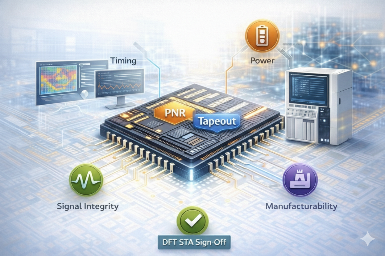
Our physical design services cover full-chip and block-level implementations across complex SoCs and high-performance ASICs. We follow structured workflows that balance timing, power, signal integrity, and manufacturability from the earliest planning stages.
Key areas of expertise include:
- Full-chip and block-level physical design implementation
- Floorplanning with macro placement and pin optimization
- Power planning and robust power distribution networks
- Standard-cell placement and timing-driven optimization
- Clock Tree Synthesis for low skew and minimal latency
- Global and detailed routing with congestion control
- Physical verification, DRC, LVS, and sign-off readiness
-
Structured Physical Design Flow
Kalibroida follows a disciplined and repeatable physical design flow to ensure quality at every stage of back-end implementation. Our process minimizes late-stage surprises and enables smooth design convergence.
-
In-Bound Design Checks
Before physical implementation begins, we validate all design inputs including netlists, timing constraints, power intent files, libraries, and technology data to ensure consistency and readiness.
-
Floorplanning and Power Planning
We define optimal core dimensions, place macros strategically, and design efficient power grids that support performance goals while maintaining power integrity across operating modes.
-
Placement and Optimization
Standard cells are placed with timing awareness, followed by multiple optimization iterations to meet setup, hold, and congestion requirements.
-
Clock Tree Synthesis
Balanced clock networks are built to reduce skew, improve clock latency, and ensure reliable timing closure across all operating corners.
-
Routing and Timing Closure
Global and detailed routing are performed with careful attention to signal integrity, crosstalk, and routing congestion, followed by final timing optimization.
-
Sign-Off and Tape-Out Support
We perform comprehensive sign-off checks including static timing analysis, IR drop, EM analysis, and physical verification to ensure tape-out readiness.
Performance, Power, and Signal Integrity
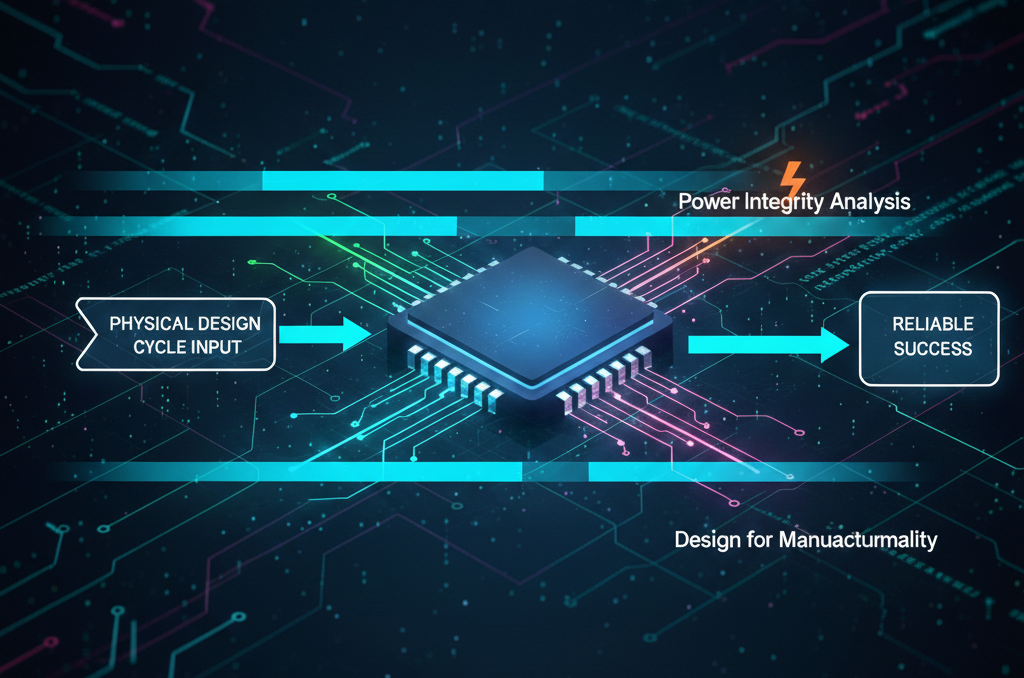
Achieving reliable silicon requires careful analysis beyond placement and routing. Kalibroida integrates performance, power, and integrity analysis throughout the physical design cycle.
Our focus areas include:
- Static timing closure across all modes and corners
- Power integrity analysis including IR drop and electromigration
- Signal integrity checks for noise and coupling effects
- Design for Manufacturability to improve yield and reliability
Why Choose Kalibroida
Kalibroida brings a strong combination of technical depth and practical execution to physical design. Our engineers understand the trade-offs required to meet PPA targets while maintaining schedule and quality.
Reasons clients choose Kalibroida:
- Deep expertise in advanced-node physical design
- Proven back-end design methodologies
- Close collaboration with front-end and verification teams
- Focus on predictable outcomes and silicon success


From Netlist to Silicon Success
Whether you are building a complex SoC or a performance-critical ASIC, Kalibroida’s physical design services provide the expertise needed to bring your design to silicon with confidence. Connect with our team to discuss how we can support your physical implementation and tape-out goals.
Get Started with Kalibroida
Kalibroida’s physical design expertise helps you optimize for speed, power, and area with predictable results.