
Kalibroida delivers industry-grade Design for Test (DFT) services built to ensure high test coverage, low test times, and robust production testability for complex semiconductor designs. With specialized expertise in test architecture, scan insertion, ATPG pattern generation, and test validation, our engineers help you embed testability into RTL and gate-level designs, ensuring silicon is not only high quality but also manufacturable and cost-effective.
DFT Architecture and Planning
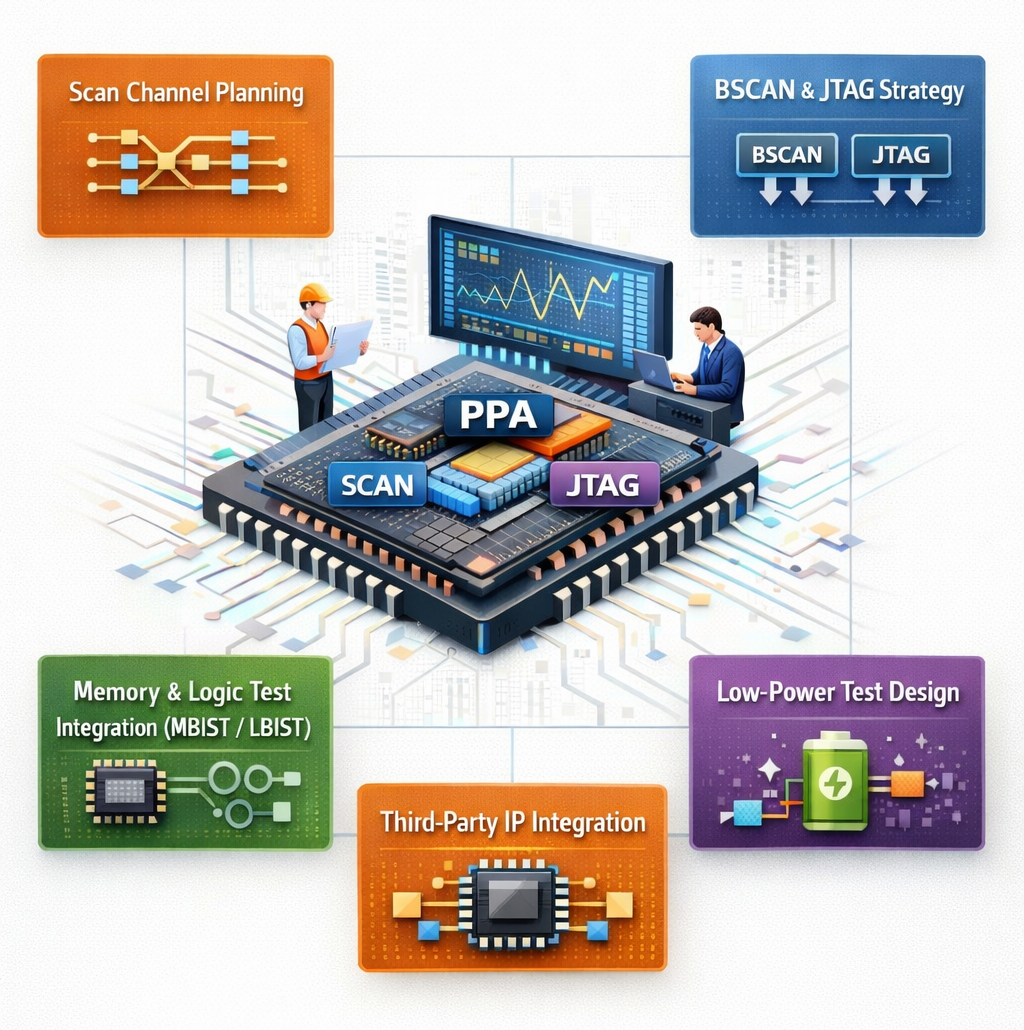
Effective DFT begins with a strong architectural plan. Kalibroida collaborates closely with your design team to define the test infrastructure required to meet coverage, speed, and manufacturability goals. We focus on creating a practical, hierarchical DFT blueprint that aligns with power, performance, and area (PPA) targets while enabling efficient test execution.
Key DFT architecture activities:
- Scan channel planning, pin usage optimization, and block-chain allocation
- BSCAN, JTAG, and hierarchical scan chain strategy
- On-chip memory and logic test integration planning (MBIST/LBIST)
- Low-power design considerations for test modes
- Third-party IP integration planning for DFT compatibility

DFT Implementation & Scan Insertion
Kalibroida’s implementation phase embeds the necessary test logic into your design while preserving functional integrity and PPA targets. Our team uses industry-standard EDA tools and scripts to insert scan chains and other structural test insertion elements without disrupting design goals.
Implementation services include:
- Full/partial scan insertion, compression, and OCC integration
- Memory BIST (MBIST) and logic BIST (LBIST) insertion
- JTAG/BSCAN insertion and boundary scan integration
- Logic equivalence checks and block-to-top test signal stitching
- DFT rule cleanup (DRC/Lint fixes) and integration readiness reviews
ATPG Pattern Generation & Validation
After inserting test logic into the design, pattern generation is essential for verifying that the design can be effectively tested during manufacturing. Kalibroida engineers generate optimized ATPG patterns that not only maximize defect coverage but also reduce overall test time and ATE cost.
ATPG and validation services:
- Generation of structural test patterns (SCAN, MBIST, JTAG)
- Compressed pattern generation to reduce volume and test time
- Gate-level simulation of generated patterns (zero delay and timing)
- Test coverage analysis and iterative improvements
- Pattern delivery, debug, and post-silicon validation support

DFT Constraints and STA Sign-Off
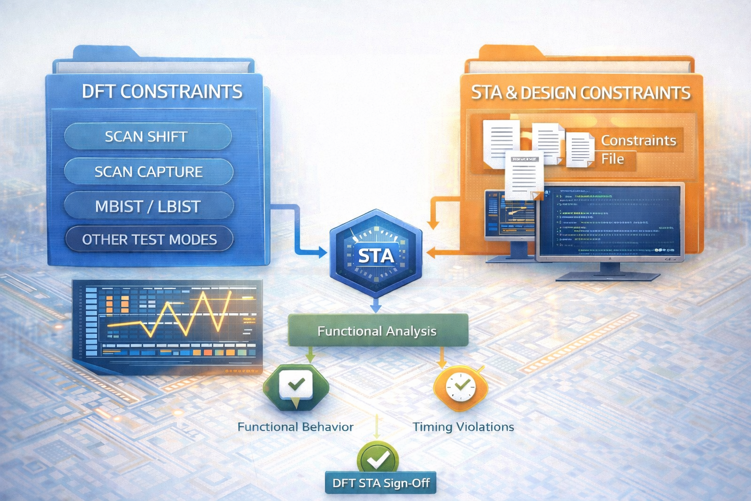
Design for Test requires careful interaction with Static Timing Analysis (STA) and design constraints. Kalibroida helps define and incorporate DFT-related constraints to ensure that test modes (scan shift, capture, MBIST modes, etc.) are accurately reflected in timing and functional analysis.
Constraint support includes:
- Test mode definitions (scan shift/capture, MBIST, JTAG modes)
- Power-aware timing constraints and test clock domains
- STA sign-off readiness for DFT logic
- Integration with low-power and clock gating strategies
Post-Silicon Test & Debug Support
Once test patterns and infrastructure are delivered, post-silicon validation helps ensure manufactured silicon meets test expectations. Kalibroida offers support for pattern debug, tester handoff, and yield improvement activities.
Post-silicon services include:
- Pattern debug and ATE handoff support
- Test log analysis and fault diagnosis
- Yield enhancement strategies
- Test program optimization for production test flow


Why Kalibroida for DFT
Design for Testability is a critical aspect of semiconductor quality and yield. Choosing Kalibroida for DFT services ensures you benefit from expert planning, seamless integration, and robust test execution strategies aligned with industry best practices. Our team’s experience with ATPG, scan technologies, and post-silicon test flows helps reduce risk, improve test coverage, and accelerate time-to-market.
Industries & Applications
Kalibroida’s DFT services are applied across high-complexity domains including automotive, industrial systems, wireless communications, multimedia SoCs, and secure embedded platforms. We deliver scalable DFT strategies for designs of all sizes—from high-density ASICs to advanced SoCs requiring hierarchical and compressed test flows.
Get Started with Kalibroida
Ready to build testability into your next semiconductor product? Contact Kalibroida to discuss how our Design for Test (DFT) services can improve test coverage, lower test costs, and deliver high-quality silicon you can trust.